Digital and Memory Controllers
Computers are logic machines. They continuously evaluate input and created desired output. Most computers rely on Central Processing Units (CPUs) and Arithmetic Logic Units (ALUs) that are created with large logic gate networks. But there is another option. For some applications it is possible to use a memory chip instead. Logic networks take some inputs and give a desired output. Using this same idea, we can apply inputs to the address lines of a memory chip, and use the data lines as the outputs. We just need to program the memory locations associated with the different address line inputs with a value that gives the desired outputs on the data bus.
Let’s look at a simple example.
Let’s look at a simple example.
|
A seven segment display is a common way for displaying numeric data. They are constructed with 7 Leds that can be lit in different patterns to display numbers and some letters. We see them all over in digital clocks. One of the issues with using these devices is that there is not an easy way to convert an actual number to the Leds that need to light for that number to be displayed. Luckily, there is a logic integrated circuit chip that can do this for us.
|
|
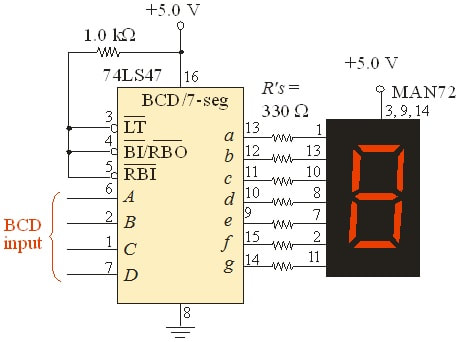
From the diagram, you can see that the 7447 (the low power LS version of the chip is shown) takes a digital number in the form of a 4-bit binary coded decimal input. Its internal logic then powers the corresponding segments to light the inputted number on the display.
Since the whole function of this chip is to take a set of inputs and generate a given output, it looks like a good candidate for replacing with a memory chip. Let’s see what that looks like.
Since the whole function of this chip is to take a set of inputs and generate a given output, it looks like a good candidate for replacing with a memory chip. Let’s see what that looks like.
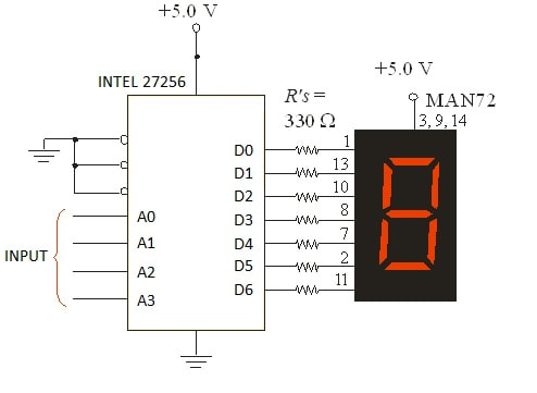
Here, we replace the 7447 with a memory chip. We use the first 4 address lines (A0-A3) as the input and the data lines (D0-D6) as the outputs to the 7 segment Led.
Now all that is left is to program the correct outputs for the given inputs. This is pretty easy since we only have 16 possible inputs (a 4-bit binary number creates 16 possible states).
Now all that is left is to program the correct outputs for the given inputs. This is pretty easy since we only have 16 possible inputs (a 4-bit binary number creates 16 possible states).

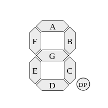
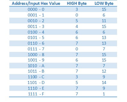
A 7-segment Led uses the designations A-G as the segments as shown. We will assign D0 to A, D1 to B, D2 to C, and so on. Whenever an input is received that requires a segment to light, we will set those data lines high. For example, for an input of 2 (address 0010), we would need to light segments A, B, G, E, and D. So we will store the value 1011011 (HEX 5B) into memory location 0010 (HEX 02). If we do this for all possible combinations (16 total), we will have a complete controller. Unlike the 7447 which is a decade (base 10) counter, we will include the HEX values above 9 to make this a true HEX to 7-segment display decoder. Here are the rest of the values.
If you have the equipment, program the data into the memory chip.
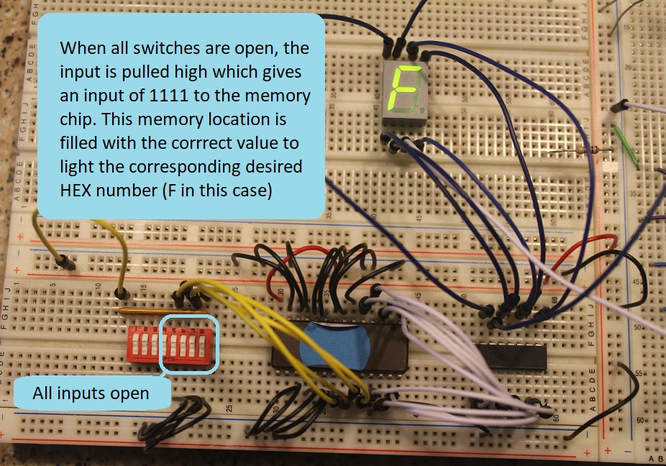
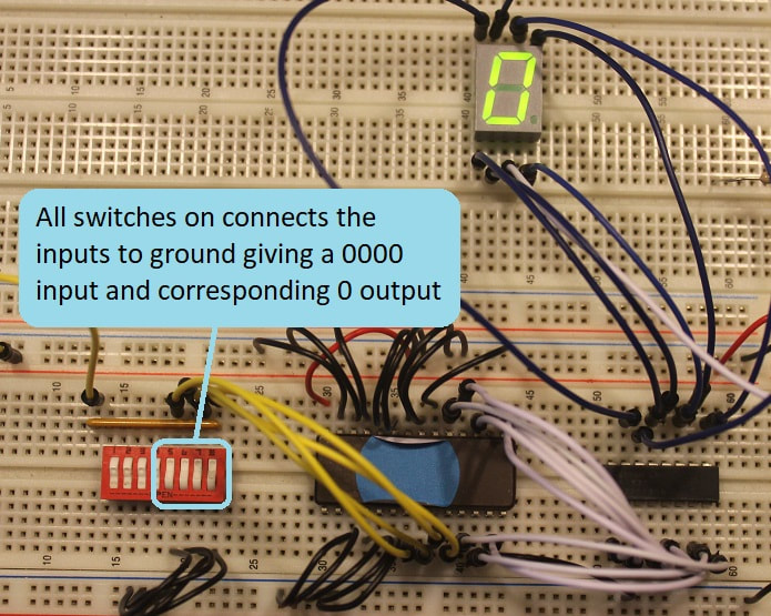
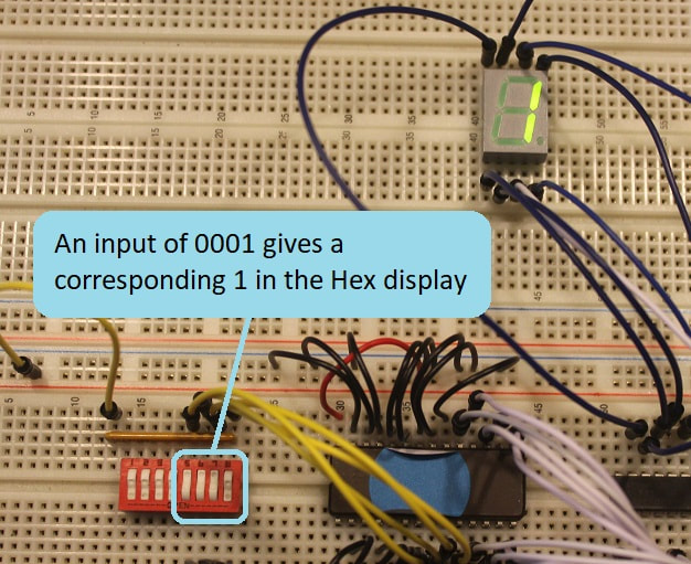
Set up the circuit as in the previous schematic. I used switches to simulate the inputs on the address lines. When the circuit is powered up, the value present at the input (A0-A3) will show up on the 7-segment display.
Set up the circuit as in the previous schematic. I used switches to simulate the inputs on the address lines. When the circuit is powered up, the value present at the input (A0-A3) will show up on the 7-segment display.
|
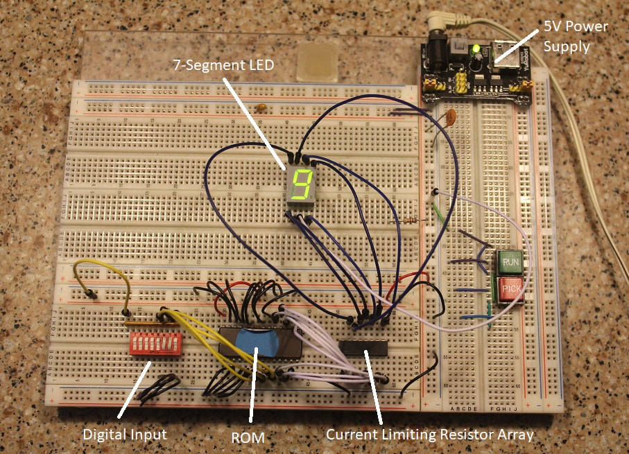
I set up the circuit on a large breadboard. In the upper right corner, there is a 5V power supply that is powering the associated power strips on the breadboard. The digital switch array is being used as the input to supply either 5 volts (high signal or logic 1) when the switch is open or 0 volts (low signal or logic 0). This is accomplished by using a pullup resistor array tied to the 5V supply. Only the right 4 switches are used. Those switch values are sent to the ROM address lines A0-A3. All other ROM address lines are tied to GND to ensure they are zero input values. The data output lines (D0-D6) are then sent to a current limiting resistor array. As a practice, I do not normally connect LEDs to chip outputs without some form of resistance in series. LEDs are, after all, diodes. When forward biased, diodes drop a very specific voltage (normally around 2-3 volts). When you hook something that drops 3V to a 5V line, something has to drop the remaining 2V. Normally, the increased current in the chip will cause a drop in the output to match the diode voltage. But I never like relying on this so I usually use a small resistor in series with the LEDs to drop the difference in voltage between the chip output and the diode. You can see from the picture that the circuit is powered and the switches are inputting a 1001 to the ROM chip which is presenting a 6E hex output on the data lines which in turn is producing the number nine to be displayed. Below are some other variations.
|
|
|
|
You can extend this example to an even more complicated example. Let's look at what it would take to make a computer Arithmetic Logic Unit (ALU).
An ALU is the part of a computer that performs certain arithmetic and logic operation like addition, subtraction, logical OR, and logical AND. For most computers, this is a complicated array of logic gates that takes the inputted numbers, evaluates the desired function, and presents the results back to the central processing unit. Since this is a state machine that takes inputs and translates them to outputs, we can substitute our memory chip and just program the desired information.
An ALU is the part of a computer that performs certain arithmetic and logic operation like addition, subtraction, logical OR, and logical AND. For most computers, this is a complicated array of logic gates that takes the inputted numbers, evaluates the desired function, and presents the results back to the central processing unit. Since this is a state machine that takes inputs and translates them to outputs, we can substitute our memory chip and just program the desired information.
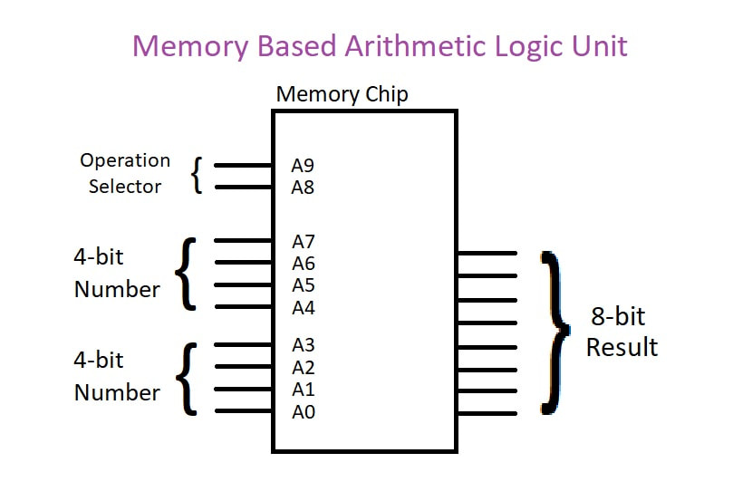
As before, we will send our inputs to the address bus and take the output off of the data bus. We will use addresses A0-A3 as the input of one 4-bit number and addresses A4-A7 as the input of a second 4-bit number. We will use addresses A8 and A9 to select the desired operation. These 2 address lines will allow us to perform 4 different operation (address inputs 00, 01, 10, 11). We can of course expand this to include more lines and consequently, more operations. Let's see how to program our controller. Let's say that operation 00 is addition. Let's program the operation of adding the numbers 0010 (decimal 2) and 1001 (decimal 9).
First we can construct the memory address created by this request.
First we can construct the memory address created by this request.
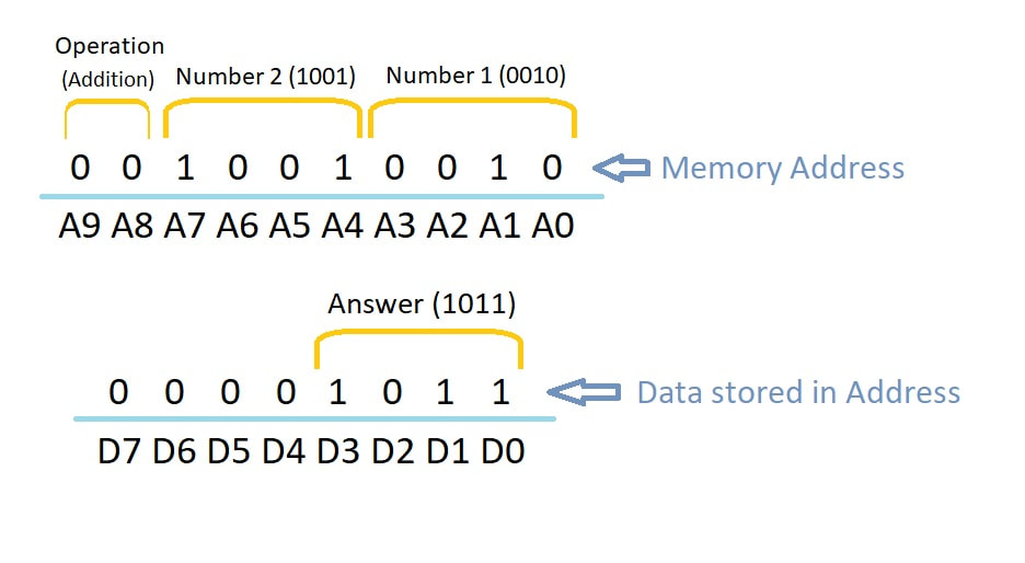
To do this, we lay out the address lines and the data lines. Then, assign the numbers to the address lines. When we read the resulting series of binary numbers, we have the address location to store the result in. We then do the math (2 + 9 = 11) so we know what value to store at this location. We then program the ROM address with this data. We know have a chip that adds these two numbers and places the result on the data lines. We just need to do every possible calculation for every other memory location and we will have a complete 4-bit ALU. That sounds difficult, but a quick spreadsheet will easily churn out these values and allow you to export the file so it may be imported into ROM writing software.
I hope you have a better understanding of memory controllers and how they can be used in place of logic circuits to perform logical state based operations.
I hope you have a better understanding of memory controllers and how they can be used in place of logic circuits to perform logical state based operations.
